On March 15, Scientific Reports of Nature publishers published the research findings of Zhou Shengjun, associate professor of School of Power and Mechanical Engineering of Wuhan University, about ultraviolet light-emitting diodes online. This research, through comparison analysis, proves that the optimum thickness of the sputtered AlN NL is around 15 nm.
This paper is entitled Effects of GaN/AlGaN/Sputtered AlN nucleation layers on performance of GaN-based ultraviolet light-emitting diodes. Doctor Hu Longpo of School of Power and Mechanical Engineering is the first author and Zhou Shengjun is the corresponding author. Doctor Hu obtained his M.S. from Tsinghua University and then became a member of Zhou Shengjun’s team on ultraviolet LED research in Wuhan University. This project is sponsored by State Natural Science Fund projects and “863” projects together with “351” talents projects of Wuhan University.
The producing of High-performance gallium nitride photoelectric devices is based on the growth of high quality GaN single crystal films, and the nucleation layer is of vital significance in its epitaxial growth process. In 1990s, Isamu Akasaki, Hiroshi Amano from Nagoya University and Dr. Shuji Nakamura from Nichia Corporation achieved the epitaxial growth of the aluminum nitride and GaN in low temperature on sapphire substrate by metal-organic chemical vapor deposition (MOCVD) technique. This contributes to the successful epitaxial growth of GaN single film in high temperature environment, marking a breakthrough in the field of UV LED. However, Zhou Shengjun discovered that when the wavelength of light-emitting diodes enters the ultraviolet band, the strong absorption on the ultraviolet light of LT-GaN nucleation layer makes it applicable in UV LEDs.
In this study, Zhou Shengjun demonstrates InGaN/AlInGaN UV LEDs grown on PSS with in-situ low temperature GaN/AlGaN NLs and ex-situ sputtered AlN NL. The UV LED in this research emits at wavelength as short as 375 nm. The comparison on the crystalline quality and the optical and electrical properties of three devices indicates that the application of sputtered AIN nucleation layer not only reduces the absorption on ultraviolet light, but also lowers the threading dislocations (TDs) density, improves the internal quantum efficiency of the device. Thereby, the luminous efficiency is increased by 30%. Compared with the conventional UV light source like mercury lamp and xenon lamp, UV LED is environment and innocuous, power saving, small in size and more lasting. This invention has attracted considerable attention for a variety of applications such as sterilization, disinfection, water and air purification, biochemistry, and solid-state lighting. Therefore, it is of particular importance for realization of highly efficient UV LEDs.

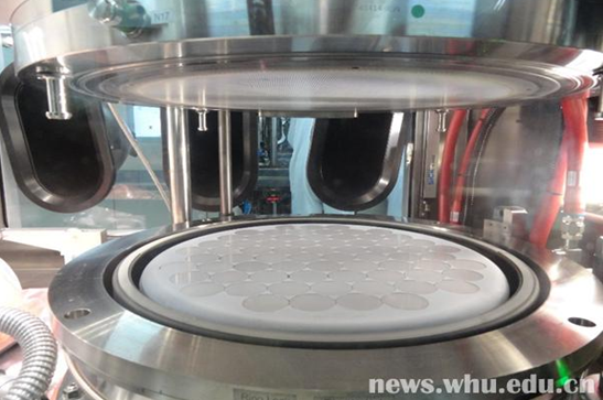
Figure 1 The MOCVD Reaction Chamber of Extended Growing Ultraviolet LED

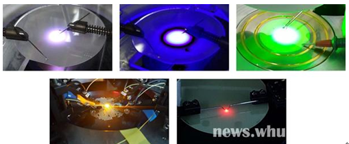
Figure 2 Fulfil Purple/Blue/Yellow/Green/Red LED by Adjusting the In Proportion of InGaN/GaN
It is known that Zhou Shengjun began his research on high-power LED chips since 2008. In 2012, he led the teams from the U.S., the U.K., Germany, Singapore and Chinese Taiwan District to do research on high-power LED chips and promote the industrialization process in Guangdong Liangjing Light Electricity Technology Co. Ltd. In 2013, they realized the large-scale mass production of 160 lm/W high-power LED chips. In the recent ten years, Doctor Zhou has made continuous research in the field of production of high-power LED chips. He has published more than 30 papers of SCI and EI indexed and has been accredited three patents.
Translated by Jin Yiwen
Edited by Shen Yuxi, Hu Sijia


